


by Roman Pletka, Nikolas Ioannou, Nikolaos Papandreou, Thomas Parnell and Saša Tomić (IBM Research Zurich)
The sustained increase in storage density and simultaneous cost reductions of NAND flash memories have ensured their continued popularity. But these positive attributes are linked to less desirable trends such as a reduction in the reliability of memory cells, requiring an increasingly overwhelming amount of sophisticated mitigation techniques, which become most apparent when applied to enterprise-level storage systems.
The continuous success of NAND flash is a result of the enormous progress achieved over the past few decades. Initially driven by the scaling of the process technology node, then assisted by an increase in the number of bits stored per cell, today, the aggressive stacking of layers in the third dimension continues to preserve this trend. Read and write operations are performed on a page granularity – where the page size is currently in the order of 16KiB – with several hundred pages being organised into a block. But an entire block must be erased prior to being programmed. Therefore, Flash controllers run a Flash translation layer (FTL), that transforms “writes” into a sequential write stream and maintains the mapping between logical and physical pages.
An increasing number of physical variables affect the reliability of NAND Flash memory cells [1]: Charge being trapped in the insulating tunnel oxide because of repeated program-erase cycling is a permanent effect that wears out cells and reduces their health, resulting in endurance limitations. Temporary effects influence the raw bit error rate (RBER) only up to the next erase operation but tend to be more pronounced as the program-erase cycle (PEC) count increases. Typical temporary effects are: (1) Cell-to-cell interference upon programming causing charge to be falsely deposited on adjacent cells due to parasitic capacitance coupling. (2) Retention limitations, where a cell gradually leaks charge after being programmed. This effect is accelerated by the amount of charge trapped, but also depends on the number of electrons stored in the cell. (3) Read disturb happens upon a read operation, where a high voltage is applied to all unselected wordlines in a block. As this voltage must be higher than the highest programmed threshold voltage, it has essentially the same effect as a tiny program impulse and therefore causes a slight shift in the threshold voltage. (4) The accumulation of static charge over time evokes an electric field that temporarily shifts the threshold voltage distributions. Only after reading a block, is the built-up charge removed. The influence on the threshold voltage distributions for the most important effects are graphically illustrated in Figure 1.
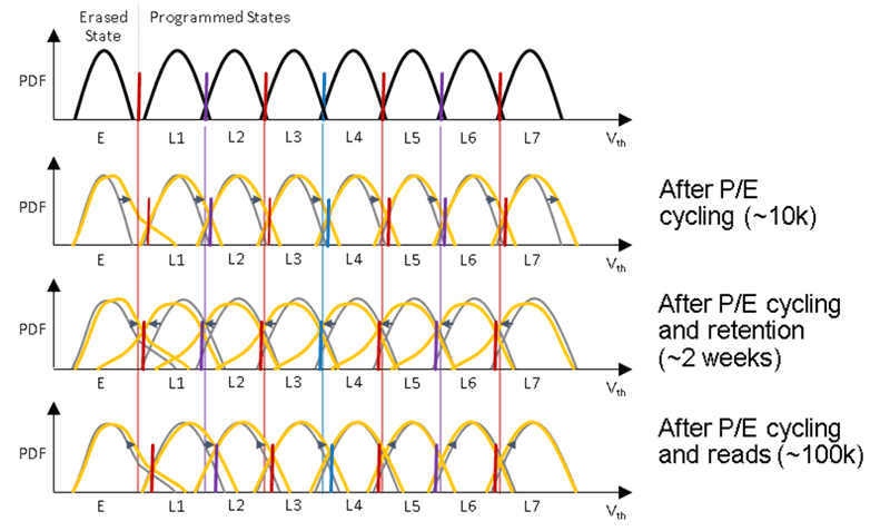
Figure 1: Effects on the threshold voltage distribution Vth of a 3-bit per cell (TLC) NAND Flash memory cell from program-erase cycling, retention, and read disturbs.
All these effects coexist in NAND Flash-based storage devices and cause widening as well as shifts of threshold voltage distributions. Today, up to four bits are stored in a single flash cell resulting in 16 charge levels that must be programmed accurately and distinguished properly upon reading. Thus, the threshold voltage distributions are very tight and tend to overlap even in fresh devices. Strong error correction codes (ECC), capable of correcting an RBER of up to 10-2 are essential to address the widening of the threshold voltage distributions but they are not sufficient.
At IBM Research - Zurich, we are exploring novel ECC algorithms and flash-management techniques that address these challenges holistically. We have developed key technologies including block calibration, a technique to determine optimal read voltage levels in the background, novel garbage-collection, data-placement, and wear-leveling algorithms that balance block health variability and – together with our hardware compressor – reduce overall write amplification.
Our technologies tightly integrate data path processing directly implemented in hardware with control path activities in firmware inside a flash card or SSD to achieve continuous mitigation in the background (Figure 2).
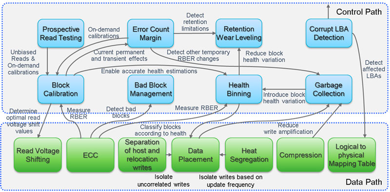
Figure 2: Overview and interactions of 3D TLC NAND flash management functions.
Because of the effects mentioned above, the threshold voltage distributions shift in different directions. Therefore, most flash memory devices support read-retry operations that apply a sequence of different threshold voltages in an attempt to lower the RBER. But consecutive reads result in a proportionally higher read latency, an unwanted effect in enterprise storage systems causing significant application-level tail latency increases.
Prospective read testing facilitates unbiased reads by ensuring that built-up charge is removed and determines blocks that need their threshold voltage shift values adapted by calibration. The block calibration engine uses the RBER measured by the ECC during background read scrubbing to determine the current set of optimal read voltage shift values [2]. The measured RBER is also used by health binning to classify blocks according to their health as well as to detect bad blocks [3]. The current permanent and transient effects on a block together with large-scale characterisation data are used to determine an upper bound of the RBER that is applied to trigger block re-calibrations and to detect early retention limitations or other excessive temporary effects on the RBER.
It has been shown that real-world workloads tend to be skewed in their access-pattern distributions. We leverage the separation of host and relocation writes as well as the segregation of writes based on their update frequency in the data placement to minimise the amount of relocated data in skewed write workloads. Both data placement and compression help to reduce internal write amplification, i.e., additional writes needed to relocate still valid data from blocks that are going to be erased such that they can be used to accommodate future writes.
At the same time, we place write hot data on the healthiest available blocks and write cold data on less healthy blocks, resulting in an efficient balancing of block wear depending on the current block state.
The compression engine, built as a streaming engine in hardware, is based on Lempel-Ziv coding combined with pseudo-dynamic Huffman codes and a 4KiB history buffer matching the logical block address (LBA) size and it can deliver inline compression at more than 1M IOPS at the system level. Finally, due to compression, a physical flash page can hold a large amount of compressed logical pages. In the rare event that the ECC cannot correct the data read, all logical pages stored in that physical page will be affected even though only a single page may have been read. Due to the log-structured organisation of data, affected logical pages are typically not adjacent and need to be detected to prevent silent data corruption. This is also applicable when data is RAID-protected by the SSD controller and there are more physical page failures than can be corrected by the given RAID level. Our algorithms allow such error events to be recovered using the array-level data protection layer and hence operate as a cooperative two-dimensional RAID scheme.
We have been able to demonstrate that using our technologies we can increase the device endurance by up to 15x without affecting performance and using acceptable additional resources only. Furthermore, we have reduced the host read retry probability by more than four orders of magnitude and lessened the tail latencies of the 99 percentiles by up to 2.7x compared to traditional wear leveling algorithms. We implemented and verified our techniques in a simulator as well as the IBM FlashSystem® all-flash array. The simulator enables us to evaluate scenarios that exceed the capabilities of the hardware environment.
IBM and FlashSystem are trademarks of International Business Machines Corporation, registered in many jurisdictions worldwide. Other product or service names may be trademarks or service marks of IBM or other companies.
Link:
https://www.zurich.ibm.com/cloudstorage/
References:
[1] Y. Cai et al., Error Characterization, Mitigation, and Recovery in Flash-Memory-Based Solid-State Drives, Proc IEEE 2017
[2] N. Papandreou et al., Using Adaptive Read Voltage Thresholds to Enhance the Reliability of MLC NAND Flash Memory Systems, GLSVLSI, 2014
[3] R. Pletka and S. Tomić, Health-Binning: Maximizing the Performance and the Endurance of Consumer-Level NAND Flash, SYSTOR, 2016
Please contact:
Roman Pletka, IBM Research Zurich, Switzerland

