


by Harry Rudin
On 17 May, IBM Research and the ETH/Z (Swiss Federal Institute of Technology at Zurich) opened the Binnig and Rohrer Nanotechnology Center on the campus of the IBM Zurich Research Laboratory in Rueschlikon, Switzerland. The name and the location are well chosen as it was here that Gerd Binning and Heinrich Rohrer invented the STM (Scanning Tunneling Microscope) some 30 years ago. They were awarded the Nobel Prize for Physics for this in 1986. The timing was also ideal as the opening helps IBM celebrate its centennial.
Binnig and Rohrer’s invention was effectively the birth of today’s nanotechnology science. There was earlier, rather scattered work at the nano-scale (ie, at dimensions in the order of 10-9 meters) but the STM and later the AFM (Atomic Force Microscope, invented by Binnig in 1985) provided the critical turning point and effectively laid the foundation for what is now the field of nanotechnology.
Nanotechnology has to do with structures with a dimension of less than 100 nanometers --- about 1000 times smaller than a strand of human hair. But working at this dimension requires rather special conditions. In fact a new building with some 6000m2 floorspace at a cost of roughly 70 million Euro was necessary to house the required equipment and researchers. This includes almost 1000m2 of clean-room facilities of the sort required for the production of the most modern integrated circuits. The facilities range from class 100 (ISO 5) to class 10000 (ISO 7). The first means that there are less than 100 particles larger than 0.5 micrometer in a cubic foot of air in the clean-room, some 10,000 times less than in the atmosphere we are used to. Temperature and humidity are carefully regulated.
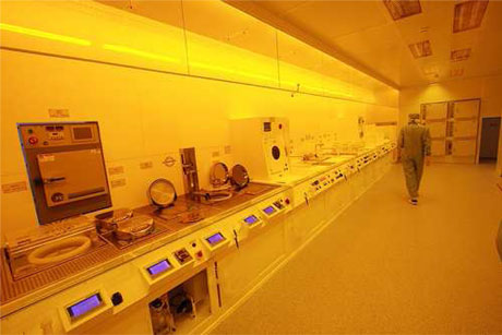
Figure 1: Clean-room facility at the Binning and Rohrer Nanotechnology Center (Courtesy of IBM Research - Zurich; unauthorized use not permitted).
The planning and construction of the “noise-free” laboratories have advanced the state of the art. Unique in the world and requiring a design task that was a substantial research effort in itself, these laboratories are necessary for the extraordinary investigations that are planned. The IBM Research designer of these facilities, Emanuel Loertscher, calls the laboratories “ultra-isolated.” The foundation rests on the bedrock below the laboratory. To further minimize the vibration there are active and passive techniques which were developed to isolate the 30- to 70-ton platforms on which the experiments will take place. This isolation reduces vibration from the rest of the laboratory, the nearby super-highway, and nearby railroad tunnel so that it remains below 500 nanometers/second. As far as acoustic noise is concerned, noise from outside the laboratories is reduced by roughly 60 db. Special shielding and dynamic electromagnetic cancelling fields reduce the alternating electro-magnetic fields to a value below 5 nano-Teslas and the static fields to a value below 20 nano-Teslas. Changes in temperature are kept below 0.1 C. per hour. The isolation is so complete that it is almost unnerving for a researcher to be in such an enclosure; the researchers sit outside of these laboratories in a less severe environment, controlling and observing their experiments remotely. Their presence in the room where the investigation takes place would severely disturb the experiment in any case.
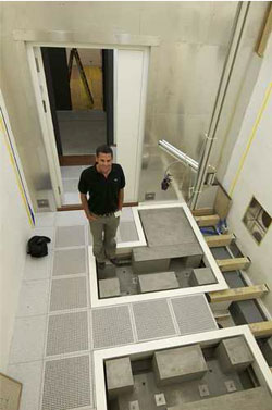 Figure 2: View of stabilized platforms for nanotechnology investigations (courtesy of IBM Research - Zurich; unauthorized use not permitted).
The nanotechnology laboratory facilities will mainly be used by researchers from IBM and the ETH although other institutions will also have use of the laboratory. Both the ETH and IBM have already produced exciting results in the nanotechnology world. For example there has been work going on at the ETH on field-effect transistors based on carbon nanotubes and investigations of the use of graphene as a basis for quantum computers. At IBM there has been work on spintronics, using the magnetic moment of electrons for computing, as well as on transistors based on nanowires and integration of photonics for communication within integrated-circuit chips. The new facilities will facilitate further work on these topics.
Looking to the future, we know that materials behave differently at the atomic level compared to their behavior at the bulk material level, creating various unique phenomena. The Center will explore these phenomena. From IBM’s point of view, a major question is what comes after the transistor. Nanowires have the advantage of very small power consumption. New display and storage technologies are also exciting topics. Bringing two groups of top-notch researchers together in a uniquely suited facility will certainly produce exciting results over the coming years, not only for nanoelectronics but also for medicine and means for environmentally friendly production.
Links:
http://www.zurich.ibm.com/nanocenter/
http://www.zurich.ibm.com/pdf/nanocenter/Nano_Center_Fact_Sheet.pdf
Please contact:
Harry Rudin, Swiss editor for ERCIM News, Switzerland
E-mail:
