


by Mario D’Acunto, Antonio Benassi, Ovidio Salvetti
Nanotechnology is the manipulation or self-assembly of individual atoms, molecules or molecular clusters into structures to create material and devices through an exact control of size and form in the nanometer scale. The immense potential of this field is presenting a challenge for the ICT world.
A nanometer (nm) is a billionth of a meter (1nm=10-9m), ie about 1/80,000 of the diameter of a human hair, or 10 times the diameter of a hydrogen atom. The term nanotechnology is generally used when referring to materials of size 0.1nm to 100nm. Materials with nanometric structures often exhibit quite different properties- mechanical, optical, chemical, magnetic or electronic - compared with traditional bulk materials made from the same chemical composition. Two principal factors cause the properties of nanomaterials to differ significantly from other materials: increased relative surface area, and quantum effects. These factors can change or enhance properties such as reactivity, strength and electricity, or optical characteristics, because the deviation of surface and interface properties from the bulk properties of larger amounts of material sometimes leads to unexpected surface effects.
Information and Communications Technology (ICT) is one of the areas that has most benefited from nanotechnologies, where it has been traditionally associated with nanoelectronics, in the efficient development and miniaturization of items such as computer chips, information storage, and sensors. Certain ICT procedures, such as distributed calculus and smart processing can be considered suitable for the implementation of bottom-up nanotechnology procedures. The self-assembly of nanostructures is the clearest evidence of a bottom-up processing (as opposed to miniaturization that can be considered the basic top-down procedure). Self-assembly is the art of building by mixing. Chemists have been doing this for centuries. The challenge today is to make such systems smart. In order to successfully use self-assembly to build micro- and nano-devices it is important to use building blocks that can be programmed to assemble in certain, pre-determined ways. If all the components that are being assembled are of the same kind, a simple over-scale structure will be the result. Using building blocks with differentiated binding sites that only fit together in certain patterns is a way to program the assembly process and makes it possible to build far more advanced structures than just periodic ones. Such processes are known as programmable self-assembly.
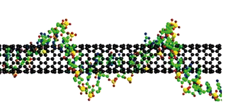
Figure 1. Example of DNA wrapping a carbon nanotube. The chemical bonding of nanotubes is composed entirely of sp2-bonds, similar to those of graphite. These bonds provide nanotubes with their unique strength, and other specific physical-chemical properties, selectively changed by the bonding with DNA filament.
One important example of programmable self-assembly is the mechanism of single stranded DNA hybridization on different surfaces, gold nanoparticles surfaces, carbon nanotubes, etc. DNA is an excellent self-assembly glue since it is specific in its bonding interactions and can be used in various nanotechnology applications, see Figure 1. Recently, we showed that the hybridization of DNA on a single-wall carbon nanotube (SWNT) is accomplished by a band-gap fluorescent shift due to changes in the exciton population (M. D’Acunto, S. Colantonio, D. Moroni, O. Salvetti, Journal of Modern Optics, 57, 1695-1699, 2010). An exciton is a bond state between an electron crossed on the conduction band and its corresponding hole in the valence band connected by the electrostatic Coulomb force. The possibility to tune the exciton population during the self-assembling process opens the road for the production of smart biosensors with many possible applications (genetic diagnosis, screening of genetically modified food, etc.). The smart biosensors, engineered by our simulations, will implement DNA sequences that are complementary to the carbon nanotubes and are compatible with specific biosensor enzymes for many different compounds. In turn, it will be a self-assembling guided procedure for biosensors at the biomolecular level. Such smart sensors could be strongly improved using graphene sheets instead of carbon nanotubes, because of the large area for single strand DNA functionalization made available by graphene sheets, see Figure 2. The construction of a smart nano-biosensor based on the self-assembly of DNA on graphene sheets is a future exciting challenge for scientists bridging the gap between the behavior of matter on the nanoscale and the ICT world. Another possible application that we are studying is to use electrospun nanofiber for hybridizing single stranded DNA. Electrospinning is a well-developed process used to produce nanofibers from a variety of materials. In electrospinning, a high voltage is applied to viscous solution on a sharp conducting tip, causing it to form a Taylor cone. As the electric field is increased, a fluid jet is extracted from the Taylor cone and accelerated toward a grounded collecting substrate. Nanofibers (having at least one dimension of 100 nanometer (nm) or less) exhibit special properties mainly due to extremely high surface to weight ratio. Within this main nanoICT challenge, we are now working on simulating possible improvements of DNA-functionalized nanofibers to be used as smart nanobiosensors through a combination of selective DNA chemical bonding with nanofiber surface.
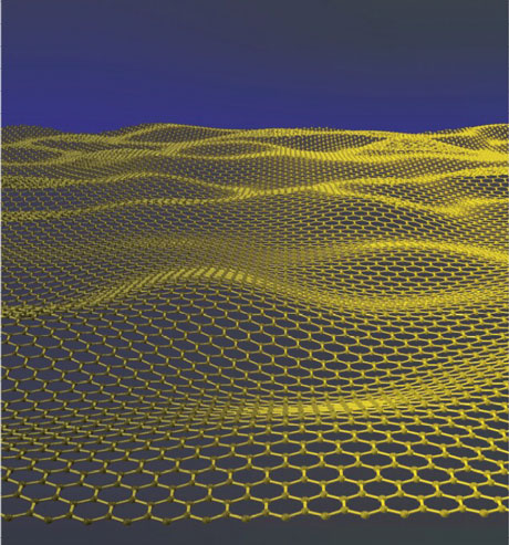
Figure 2: A graphene sheet: a one-atom-thick planar sheet of sp2-bonded carbon atoms densely packed in a honeycomb crystal lattice. The crystalline or flake form of graphite consists of many graphene sheets stacked together.
Please contact:
Mario D’Acunto, ISM-CNR, Italy
E-mail:
Ovidio Salvetti or Antonio Benassi, ISTI-CNR, Italy
E-mail:
