by Haralampos Pozidis, Nikolaos Papandreou, Thomas Mittelholzer, Evangelos Eleftheriou (IBM Research Zurich)
We are entering into an exciting era for data storage and memory, and as a consequence, computing as a whole. Next-generation, revolutionary memory technologies are at the advanced development stage in semiconductor fabs around the world and promise to enable new applications in the near future.
Memory and storage technologies have always been at the core of information technology and have enabled huge leaps in the efficiency, performance and usability of computing systems. Two of the most prominent examples are DRAM (dynamic random access memory) and Flash memory, both of which revolutionized the way computers interact with and process data. In the past several decades both DRAM and Flash have been riding the exponential growth curve offered by the continuous reduction of the semiconductor technology node, fueled by steady advances in lithography. However, lately, both technologies have been experiencing a scaling slow-down. DRAM devices with 8Gbit die capacity have only recently been announced, whereas for NAND Flash the lateral scaling has stopped at the 15nm node and exploration of three-dimensional stacking has begun in order to maintain density growth.
In the quest for high memory density, low latency and storage-like cost, all major semiconductor manufacturers have invested in the research and development of new materials and devices with better scalability prospects than conventional ones. As a result of these efforts, in the past decade or so, we have witnessed the emergence of several new memory technologies. The exciting new prospect of most of these memories is that they exhibit "universal" properties, i.e., properties akin to both main memory and storage. On one hand, these memories can be written and read fast, have very high write endurance, can be written in place and have byte-level granularity, making them suitable for main memory applications. On the other hand, they are nonvolatile and can be manufactured at very high density, which are typical characteristics of mass storage devices.
The promise of universal memories lies not only on their superior scalability potential, but also on the prospect of enabling a whole new set of applications that are rapidly emerging in the fields of databases, analytics processing and big data in general. This is mainly because of the possibility of offering memory devices with very large storage capacity, and latency close or similar to that of DRAM. Such a capability could enable such tasks as keeping entire databases in memory and processing queries in real time, without the need for complex cache hierarchies and cache management policies. Similarly, analytics on very large datasets could also be run considerably faster, without the performance penalties associated with disk or Flash accesses.
One of the prominent universal memory technologies is the so-called phase-change memory (PCM). PCM is based on chalcogenide alloys, i.e., alloys containing elements of group VI of the periodic table (such as Se or Te), typically combined with group IV/V elements (such as Ge, Sn, As, Sb). These materials exist in two phases, a highly conductive, poly-crystalline state and a highly resistive, amorphous state. Transition between the two phases is achieved by heating the material using electrical pulses in a nanoscale memory cell consisting of a phase change material placed between two electrodes. The two material phases exhibit drastically different electrical resistance and can be used to store 1 bit of information (logical 0 or 1).
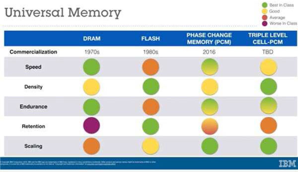
A key requirement for PCM (or any other universal memory) to become competitive with incumbent memories and to eventually enter the market is the cost per bit of the technology, which needs to be at least lower than that of DRAM. One common way to reduce the cost per bit is to increase the memory density by storing multiple (more than one) bits per physical cell. One big advantage of PCM is that it is, in principle, highly amenable to multi-bit storage, because of the large (typically 3-4 orders of magnitude) resistivity contrast between its two extreme phases. A relative comparison of existing memory technologies with PCM is shown in Figure 1.

Figure 1: Relative comparison of memory technologies in terms of main characteristics.
Multi-bit storage in PCM is achieved by forming intermediate states which represent different degrees of partial crystallization within the phase change material volume. However, a number of reliability issues hamper the realization of multiple bits per cell in PCM devices. In particular, two of the predominant issues are the instability of the electrical conductivity of the material with time elapsed after programming (resistance drift) and the sensitivity of the stored states to ambient temperature variations. Both of these phenomena are exacerbated by increasing the number of bits stored in a cell, because the signal margin between adjacent states is then reduced.
Our work at IBM Research - Zurich has been focused on finding effective solutions to the above problems and thus enabling reliable multi-bit storage in PCM. Specifically, we have developed three key technologies for that purpose. The first is a novel metric that is used to read the information stored in a PCM cell that is almost invariant to resistance drift, i.e., exhibits significant stability over time. Conceptually, this new metric measures a quantity akin to the proportion of amorphous phase material within the volume of the PCM cell, which is stable over time in contrast to the electrical resistance that is varying. The second technique is a signal processing scheme that adapts the level detection thresholds placed between signal states in such a way as to always guarantee the best possible distinction between adjacent states, despite any resistance variations due to drift or temperature changes. Last, but not least, a novel coding scheme shapes the data stored in the PCM cells so that information is stored not on the actual signal levels, but on their relative order within a collection of cells, called a codeword.
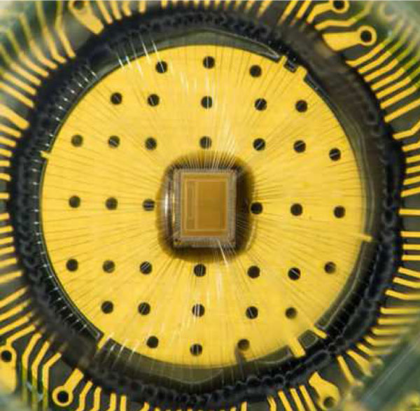
The judicious combination of the above three innovations has been instrumental in addressing all the major reliability concerns in multi-bit PCM. In particular, we have been able to demonstrate, for the first time, highly reliable data storage at 3bits/cell density in an array of 64 kcells that have been pre-written 1 million times [1] (Fig. 2). Furthermore, we demonstrated successful retention of the stored data over a period of 10 days in the presence of ambient temperature variations between 25 and 75 degrees Celsius. These results help establish the practical viability of multi-bit PCM, which has always been considered a difficult problem, and pave the way for truly competitive PCM products with new promising applications.

Figure 2: Close-up picture of a phase-change memory chip used in the 3bits/cell demonstration.
Our current work centers around the exploitation of PCM technology in future computing systems, in particular storage systems and servers. As a first step, in collaboration with the University of Patras, in Greece, we have developed a phase-change memory (PCM) sub-system attached to the POWER8® processor via the Coherent Accelerator Processor Interface (CAPI). The POWER8® processor architecture with its CAPI interface provides an efficient communication mechanism to PCM over the PCI Express link. In a platform comprising a POWER8® server, an FPGA card and custom DIMMs made of legacy 128 Mb PCM chips, we demonstrated 128-byte accesses from/to PCM at consistently very low latency, namely up to 3.1 µs and 8.8 µs for 99% of the write and read operations, respectively. These results were recently presented at the 2nd OpenPOWER Summit [2] and demonstrate the potential of using PCM as a fast storage tier directly attached to the processor through an I/O link.
IBM and POWER8 are trademarks of International Business Machines Corporation, registered in many jurisdictions worldwide. Other product or service names may be trademarks or service marks of IBM or other companies.
Link:
http://www.research.ibm.com/labs/zurich/sto/memory/
References:
[1] M. Stanisavljevic, et al.: “IEEE Intl. Memory Workshop”, Paris, May 2016.
[2] http://openpowerfoundation.org/presentations/low-latency-access-to-phase-change-memory-in-openpower-systems/
Please contact:
Haralampos Pozidis, IBM Research Zurich, Switzerland


