The nanoCMOS project began in October 2006 and is due to run for four years. It involves collaboration between leading device-modelling and circuit and system design research groups at the Universities of Glasgow (PI Prof Asenov), Edinburgh, Manchester, Southampton and York. This strong academic group is enhanced by robust links with industrial partners including leading tool vendors and design companies such as Synopsis, Freescale, ARM, Fujitsu, National Semiconductor and Wolfson Microelectronics among others.
The increasing device variability of CMOS devices demands revolutionary changes in the design of, and design methods for, integrated circuits and systems. To achieve this, it is now recognized that a real paradigm shift must occur and strong links must be established between system, circuit and fundamental device technology research and design groups to allow modern integrated circuits to cope with the individual behaviour of statistically varying transistors on a chip. In the past, the assumption has been that there is a single idealized transistor used across a chip, but as the scale of devices shrinks this no longer holds. Instead, design methods must evolve to accommodate the increasing statistical variability of transistors and the impact this can have on circuit and system performance.
Changing design rules for device architecture and variability adds significant complexity to the design process, requiring the orchestration of a broad spectrum of design tools by geographically distributed teams of device experts and circuit and system designers. In nanoCMOS this is being addressed by embedding e-Science technology and know-how across all nanoCMOS electronics design groups, revolutionizing the way in which these disparate groups currently work and more importantly, providing new insights for industry on the challenges faced in the nanoCMOS domain and on how the global semiconductor industry can address them.
In order to study the statistical fluctuations introduced by the atomic structure of transistors it is necessary to perform 3D simulations of huge ensembles of hundreds of thousands of devices, rather than a single representative device. Given the increasing number of transistors in modern chips, simulation of very large statistical samples of devices is required to allow statistically rare devices with potentially fatal effects on circuit performance to be examined. This demands access to huge distributed high-performance computing resources including the UK e-Science National Grid Service and ScotGrid, and a wide variety of other resources including Condor pools and campus clusters across partner sites.
However this is not simply another large-scale simulation problem, since the commercially sensitive nature of the problems and stringent IP protection demands fine-grained security on access to, and usage of, licensed software, providing protection for the intellectual property associated with circuit and device designs, data and simulations belonging to industrial partners and key stakeholders. To this end, the project has developed infrastructure that provides security throughout. This includes exploitation of Kerberos for secure global file-based access through the Andrew File System; authorization technology such as PERMIS for definition and enforcement of access policies using centralized attribute authorities such as the Virtual Organization Membership Service (VOMS); and simple user-oriented access to the project portal through the Internet2 Shibboleth technology using the UK Access Management Federation. This portal contains a variety of services for atomistic device simulation, compact model generation and circuit simulation, as well as mechanisms for managing the large and heterogeneous data and metadata associated with these simulations.


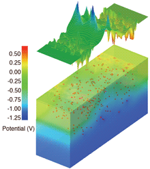
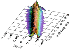
The project is now well advanced and the initial prototype infrastructure is ramping up for large-scale scientific usage. Up until now, due to the computational complexity of 3D device simulation, studies of variability have tended to be based on small ensembles of typically up to 200 devices. We have simulated ensembles in excess of 100,000 3D devices for 35nm and 13nm gate-length devices. Ensembles of this magnitude are shedding new light on the effects of atomic structure variation on the behaviour of devices, especially extreme limits of device variability. Furthermore, based on these simulations, we have been able to examine the effect of device variability at a simple circuit level and have simulated over 1 million CMOS inverters using random configurations of devices. Figure 1 shows the potential and dopant position of a statistically rare device. Figure 2 shows the threshold voltage variation as a function of the number of dopants.
The second phase of this project will use the methodologies developed to study larger and more advanced circuits and systems and to further explore the impact of atomistic variability of transistors on the design process. More information on the nanoCMOS project is available on our Web site.
Links:
UK Engineering and Physical Sciences Research Council: http://www.epsrc.ac.uk
The nanoCMOS project: http://www.nanocmos.ac.uk
UK e-Science National Grid Service: http://www.ngs.ac.uk
ScotGrid: http://www.scotgrid.ac.uk
Please contact:
Asen Asenov
(science-related questions)
University of Glasgow, UK
E-mail: a.asenov![]() elec.gla.ac.uk
elec.gla.ac.uk
Richard Sinnott
(e-Infrastructure-related questions)
University of Glasgow, UK
E-mail: r.sinnott![]() nesc.gla.ac.uk
nesc.gla.ac.uk


