by Cyriel Minkenberg, Ronald Luijten and Francois Abel
Optics offer significant potential as the communication infrastructure of choice for future supercomputers. The exploratory OSMOSIS project has resulted in a prototype of an electronically controlled optical packet switch with an aggregate capacity of 2.5 Tb/s. This device is designed specifically to meet high-performance computing (HPC) requirements.
Recently, the rate of progress in CPU performance has slowed down considerably, mainly because of power constraints. Nowadays, the preferred approach to increasing computer performance is to use many processors in parallel, each relatively simple and power-efficient, thus giving rise to massively parallel computer architectures with thousands or even tens of thousands of processors making up a single machine. To collectively solve a problem, these processors need to communicate among each other with low latency and high bandwidth. In such a machine, the network used to interconnect the processors is a crucial factor in determining the system's overall performance.
Optical technology holds substantial promise for interconnection networks in HPC systems for a number of reasons. First, an optical switch typically consumes significantly less power than a comparable electronic switch because its power consumption is proportional to the packet rate rather than to the bit rate; second, fibre is much better suited than copper to the transmission of high data rates over long distances; and third, optics neither generate nor are sensitive to electromagnetic interference.
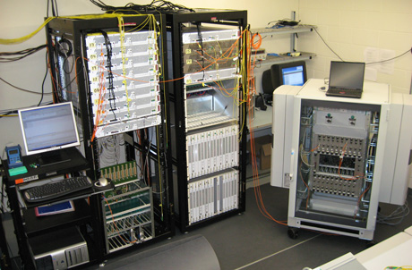
In the Optical Shared MemOry Supercomputer Interconnect System (OSMOSIS) project, Corning Inc and IBM Research have jointly explored this promise by developing an optical network switch prototype. The project was sponsored by the US Department of Energy. The result (see Figure 1) of this four-year endeavour is the highest-capacity optical packet switch in the world, with 64 ports running at 40 Gb/s, switching fixed-size packets (cells) of 256 bytes at an aggregate rate of 1.25 billion packets per second. A state-of-the-art electronic controller, which computes an optimal switch configuration once in every packet slot of 51.2 ns, ensures that throughput and reliability are maximized and latency minimized.

Optical switching has three main drawbacks, namely the absence of a practical, dense, fast-access optical memory technology, the complexity of its optical control and arbitration, and the cost of fast optical switching components. The OSMOSIS project addressed these drawbacks by adopting a hybrid electro-optical approach, using electronics to implement buffering and scheduling and optics for transmission and switching.
HPC switches must deliver very low latency, an extremely low bit-error rate, a high data rate, and extreme scalability. Moreover, they must be efficient for bursty traffic, with demands ranging from very small messages (eg collective operations and syncs) to bulk dataset transfers (eg memory pages). The main challenge for OSMOSIS was the short packet duration, which resulted in a small overhead budget of 12.8 ns for switching time, synchronization time, line coding, forward error correction and header information. This was achieved by using Corning's high-speed semiconductor optical amplifier (SOA) technology, which provided sufficiently fast switching times (< 3 ns).
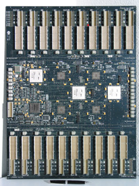
Moreover, unlike most other optical switches, which are designed to be reconfigured at a relatively slow rate using a circuit switching or container-switching approach, OSMOSIS was designed to perform just-in-time packet-by-packet switching, reconfiguring the data path every 51.2 ns. This put a heavy burden on the controller, which was addressed by IBM's novel highly distributed controller architecture. The challenge was magnified by being limited to using only field-programmable gate arrays (FPGAs) for reasons of cost and flexibility. The controller's final implementation uses a 36-layer midplane (see Figure 2) holding 40 daughter cards and a total of 48 high-end FPGAs.

The key requirement in computing systems is low latency, as latency typically translates directly into idle processor time. To meet the requirement of less than 1 ms latency measured application-to-application, we designed novel control algorithms to reduce latency by up to 50%. Further requirements for our prototype system included a bandwidth efficiency of 75% user payload, a maximum link utilization of at least 95%, a bit-error ratio less than 10-21, and scaling capability to support more nodes (>= 2048) and higher line rates (>= 160 Gb/s).
The OSMOSIS project has demonstrated the viability of SOA-based optical packet switching. It is the first system-level optical packet switch with more than two ports operating at 40 Gb/s that does not resort to container switching.
OSMOSIS also sports a number of architectural and algorithmic innovations. For instance, it uses a combination of a speculative transmission scheme with dual receivers per output to significantly reduce latency. Its deeply pipelined controller architecture uses multiple independent scheduling engines in parallel to achieve high utilization. Its highly distributed nature allows physical distribution across multiple FPGA devices to manage complexity. At the heart of the controller is one of the world's most complex board designs (36 layers, 13,000 wires, 45,000 connections), which was awarded a Mentor Graphics PCB Technology Leadership Award. It also features one of the highest concentrations of high-end FPGAs in a single system.
To make the OSMOSIS switch architecture commercially viable and fit for practical deployment, drastic cost reductions through dense integration of optical components and ASIC (application-specific integrated circuit) integration of controller logic will be needed. The critical technology to make this level of integration cost-effective is already under development.
This research is supported in part by the University of California.
Link:
http://www.zurich.ibm.com/~fab/Osmosis/
Please contact:
Cyriel Minkenberg, IBM Research, Switzerland
E-mail: sil![]() zurich.ibm.com
zurich.ibm.com


